


For those unfamiliar, Intel follows a "tick tock" model for its processor upgrade cycle. With every "tick" the company moves to a smaller manufacturing process, from 32nm to 22nm in this case, dramatically increasing transistor density while enhancing performance and energy efficiency of the current microarchitecture. Then, with an alternating "tock" cycle Intel introduces a new processor microarchitecture.
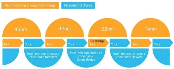
Ivy Bridge includes manufacturing and subsystem improvements. It is a shrink of Sandy Bridge and is also the first to us Intel's Tri-Gate transistors, which use a nonplanar architecture to cram more transistors into less space, therefore consuming less power or delivering more performance within the same power envelope.
There's been quite a bit of information on Ivy Bridge going around ever since Intel detailed the architecture late last year. We'll recap some of the major changes and practical implications, while also bringing you up to speed on the latest developments, including expected launch lineup and pricing.
Techspot